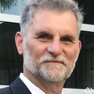
Semiconductors and 3D Stacking Expert Witness | Vermont
Semiconductors and 3D Stacking | E-528448
Expert Qualifications
This highly qualified expert has over 20 years of experience in his field, with demonstrated experience with semiconductors, ROM, DRAM, SRAM, 3D stacking, and signal interfaces. He earned his BA in electrical engineering at Union College before completing his MS in electrical engineering and PhD in material science at the University of Vermont. He has he's several roles throughout his career including being a senior research and development scientist at IBM Microelectronics, the director of technical marketing at Innovative Silicon Inc., the IP strategy director at Rambus Inc., and the memory development engineer at Invecas Inc. Most recently, he served as an adjunct professor of semiconductor physics at the University of Vermont.
Bio Snapshot
Located: VT
BS, Electrical Engineering, Union College
MS, Electrical Engineering, University of Vermont
PhD, Material Science, University of Vermont
Former, Senior Engineer, IBM Corp.
Former, Manager, Stacked DRAM Product Development, Irvine Sensors Corp.
Former, Senior Research and Development Scientist, IBM Microelectronics
Former, Principal, CellularRAM Concept Engineer, Qimonda DRAM Design Center
Former, Director, Technical Marketing, Innovative Silicon Inc.
Former, IP Strategy Director, Rambus Inc.
Former, Memory Development Engineer, Invecas Inc.
Former, Adjunct Professor, Semiconductor Physics, University of Vermont
